Understand why the usage rate of silicon wafers is one of the factors that most interferes in the price of products that reach the consumer
The usage rate of silicon wafers is, in short, the percentage of failures presented on chips mass produced from a silicone mold. The higher the usage rate, the greater the number of “perfect” chips per batch, and this proportion directly affects the prices of the products that will use those chips.
- What is the utilization rate of silicon wafers?
- What is silicon and why are microchips made from this material?
OR Canaltech I spoke to the applications engineer at Intel Brazil, Yuri Daglian, on what the usage index is and we inevitably come across the impacts of this factor for the final consumer.
“To make any type of product viable, it needs to have volume, and I need to think about the defect rate in my production. No process has 100% utilization, defects will occur. So, knowing this, I can create a design for my high-end chip, with all cores present and leaving, within this design, some tolerance of the following type: if there is a defect affecting 2 colors, I can still use this chip, it just won’t work if it will be high-end, it will be mid-range,” explained Yuri Daglian.
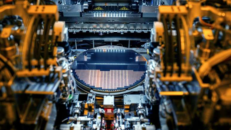
Silicon wafer prices
Briefly revisiting what we have already seen about usage rates, the production of modern chips involves a extremely complex and, above all, expensive process. However, this cost itself goes far beyond just the production line and involves all the investments in research and advanced equipment, such as advanced microlithographic scanners.
In practice, these machines emit very high frequency light beams, well above the ultraviolet range, hence the name Extreme ultraviolet. This light passes through masks equipped with chip “molds”, “printing” the entire set of circuits on the silicon appropriately prepared and treated to react to the irradiation process.
However, as Yuri explained, no large-scale manufacturing process is free from defects. They will always occur, to a greater or lesser extent, depending on several factors, including:
- Circuit dimensions: The smaller the printed components, the more precise the microlithography process needs to be.
- Circuit complexity: Very complex circuits are more prone to failures
- Architecture maturity: By identifying critical points in processes, manufacturers tend to optimize them, and brand new architectures have not yet had enough time for observation and experimentation in large-scale manufacturing to identify these potential flaws.
- Maturity of embedded technologies: the same applies to the type of technologyas the transistor standard used.
- Input quality: The very quality of the silicon used in the manufacturing of the wafers affects the potential reactivity of the wafers to the microlithography process, fatally interfering with the final product.
- External interference: Although foundries are extremely controlled environments, the process itself is extremely sensitive and involves working with very high frequency light irradiation. A change in voltage, however imperceptible it may be in normal processes, can change the frequency of the beam and cause circuit print failure.
You still need to always add chips to your account e investments in Research and Developmentstudies, tests, quality control, exchange of technologies and professionals, and so on.
Therefore, each new generation of chips, be they CPU, GPU, NAND memories or any other semiconductor-based component, is always and invariably priced with the aim of covering all costs – and still generating profit – on the flagship design. In other words, the cost of producing the new Meteor Lake chips depends entirely on the chips Intel Core Ultra 9 185Hat the top of the range with the lowest possible failure rate in the final design.
“Depending on the level of my defects, I can still exploit this processor, but at a slightly lower performance level. Of course the end consumer will also pay less. I plan this into my project from the beginning, assuming that a defect, I already prepare my processor so instead of having to discard all the defective chips, I only have to discard 20% of them, use 10% in the high-end and the remaining 70% in slightly more entry-level products.”
One wafer for every wafer
In parallel, it is important to reinforce the fact that, unlike the old monolithic chips, the new chiplet standards are equipped with chiplets advanced packaging like Intel Foveros, are not composed of a single wafer. This is because, due to the manufacturing process itself, each of these silicon wafers uses a “mask” specific to each wafer.
The Core Ultra 9 185H design uses a number of different wafers, in different lithographs, with different architectures, being a for each chiplet that make up the processor. The immediate benefit of this approach is that more mature architectures tend to have higher wafer utilization, as well as a lower manufacturing cost.
“Costs [de fabricação] they are increasing exponentially, so we need to think about alternatives, such as disaggregated architecture, which we call packaging here. It’s the act of being able to produce different positions on the chip in different lithographs, putting it all together and having a working chip. The larger the tablet I have to produce at one time, the easier it will be to have a defect. If I make the processor with very small chips and then put everything together, the chance of a manufacturing defect is much lower than if I made a processor of the same size, but in monolithic form.”
This allows you to dilute the cost of the entire project, since the most modern and expensive microarchitectures will be used only in the components for which they are indispensable. If there was no upgrade of a specific group of accelerators between generations, the new generation will still use that cheaper chiplet with better performance.
Portfolio starting from the top
In short, the computational design of a processor Raptor Lake Update i9-14900K and an i5-14600K it’s the same from end to end, from the research and development phase to the assembly line. Pricing is set based on all these costs, marketing, expected profit projections and average usage rate of this generation’s wafers, already considering what will be lost and what will be used in high-end chips.
We have another type of training to talk about this March 🤔
Which Intel solution helps spark innovation in your life? Tell us about it ⬇️ pic.twitter.com/akBL3vPOHC
—Intel (@intel) March 21, 2024
“This process is extremely important to enable economies of scale and to be able to provide good products with a high level of quality, but at a lower cost to my end customer.”
From there, the remainder of the portfolio is built up and priced as a percentage of the value of the most expensive product relative to the estimated performance of each segment. For this reason, manufacturers generally have the habit of launching high-end products first, then intermediate ones and only entry-level products last.
It is worth noting that this is a practice in the entire semiconductor industry and it is not limited to PC processors, but also extends to video cards, smartphones, consoles and so on.
- 🛒 Buy Intel Core processor at the best price!
- 🛒 Buy gaming notebooks with Intel Core CPU at the best price!
Trends on Canaltech:
- It is FALSE that the Earth will be “much further” from the Sun! Understand what aphelion is
- The 50 funniest Google Assistant jokes
- The 20 best horror films of the new generation
- 😱 ANOTHER FALLEN | Buy Galaxy S23 Ultra 256 GB at an unmissable price
- Samsung Q60D Review | QLED TV with good value for money
- iPhone starts vibrating without warning and bothers users
Source: Terra
Rose James is a Gossipify movie and series reviewer known for her in-depth analysis and unique perspective on the latest releases. With a background in film studies, she provides engaging and informative reviews, and keeps readers up to date with industry trends and emerging talents.

![Tomorrow belongs to us in advance: Violet takes risks… What awaits you in the week of October 20-24, 2025 [SPOILERS]](https://fr.web.img6.acsta.net/img/84/4f/844fc0f4a394a4dbfcf4dfd7a5d3fe41.jpg "Tomorrow belongs to us in advance: Violet takes risks… What awaits you in the week of October 20-24, 2025 [SPOILERS]")

